techniques are used for RF PCB grounding
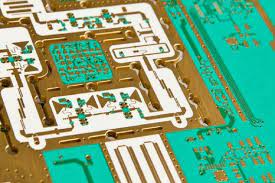
RF PCBs operate at much higher frequencies than most other electronic circuit boards, so they require special attention to detail when it comes to grounding. This is important to prevent EMI and to ensure that signal currents do not build up in areas of the board that can lead to ground loops and interference. Several techniques are used for RF PCB grounding, including careful component placement, proper signal trace width and spacing, and the use of multiple layers of copper to provide an easy return path for signal currents.
Proper component placement is crucial for RF PCBs, as it allows the designer to optimize signal paths and minimize parasitic capacitance and inductance. Special consideration must be given to the placement of high-speed components, connectors, and antennas, as they are particularly prone to signal interference issues.
Getting the layout of the signal paths right is also key to preventing impedance mismatch problems that can result in signal oscillations. This can be a big problem, as it can cause the current to bounce back and forth between the sending and receiving ends of the signal, which can reduce performance.
In order to keep impedance fluctuations as low as possible, the copper on an rf pcb must be kept as thick as possible. This can be accomplished by using multiple layers of copper and incorporating via holes in the board to connect each layer.
What techniques are used for RF PCB grounding?
Another method for reducing inductance on an RF PCB is to split the ground plane into two layers. This will help to increase the distance between a signal and the ground plane, which can be helpful in eliminating ringing caused by excessive inductance on the ground traces. In addition, putting stitching vias on the ground plane can help to control resonance frequencies by creating small stubs on the ground plane that are soldered to the surrounding copper wires.
The power supply is another area that requires particular attention when designing an RF PCB. It is important to place decoupling capacitors on the power supply in order to filter out noise and protect against polarity inversions. These capacitors should be chosen with a self-resonant frequency (SRF) that is close to the noise frequency to achieve maximum effectiveness.
It is also a good idea to use short direct routed traces and vias when connecting IC chips and other parts to the ground plane, and to avoid routing across the signal path where possible. This will help to keep the signal current as close to the ground plane as possible, which will further reduce inductance and impedance variations. Lastly, it is a good idea to make sure that all connector pins are connected to the ground plane as well, as this will reduce the chance of ground loops. It is also a good idea to use separate ground pins for analog and digital signals, as these may have different impedance requirements.